- 您现在的位置:买卖IC网 > Sheet目录868 > LTM4600IV#PBF (Linear Technology)IC DC/DC UMODULE 10A 104-LGA
�� �
�
�LTM4600�
�APPLICATIONS� INFORMATION�
�The� typical� LTM4600� application� circuit� is� shown� in� Figure�
�18.� External� component� selection� is� primarily� determined�
�by� the� maximum� load� current� and� output� voltage.�
�down� when� Q� DOWN� is� on� and� Q� UP� is� off.� If� the� output�
�voltage� V� O� needs� to� be� margined� up/down� by� ±M%,� the�
�resistor� values� of� R� UP� and� R� DOWN� can� be� calculated� from�
�Output� Voltage� Programming� and� Margining�
�The� PWM� controller� of� the� LTM4600� has� an� internal�
�0.6V±1%� reference� voltage.� As� shown� in� the� block� dia-�
�the� following� equations:�
�(R� SET� R� UP� ) ? V� O� ? (1� +� M%)�
�(R� SET� R� UP� )� +� 100k�
�=0.6V�
�gram,� a� 100k/0.5%� internal� feedback� resistor� connects�
�V� OUT� and� V� OSET� pins.� Adding� a� resistor� R� SET� from� V� OSET�
�pin� to� SGND� pin� programs� the� output� voltage:�
�R� SET� ?� V� O� ?� (1–� M%)�
�R� SET� +� (100k� R� DOWN� )�
�=� 0.6V�
�V� O� =� 0.6V� ?�
�100k� +� R� SET�
�R� SET�
�Input� Capacitors�
�The� LTM4600� μModule� should� be� connected� to� a� low�
�Table� 1� shows� the� standard� values� of� 1%� R� SET� resistor�
�for� typical� output� voltages:�
�Table 1� .�
�ac-impedance� DC� source.� High� frequency,� low� ESR� input�
�capacitors� are� required� to� be� placed� adjacent� to� the� mod-�
�ule.� In� Figure� 18,� the� bulk� input� capacitor� C� IN� is� selected�
�R� SET�
�(k� Ω� )�
�V� O�
�(V)�
�Open�
�0.6�
�100�
�1.2�
�66.5�
�1.5�
�49.9�
�1.8�
�43.2�
�2�
�31.6�
�2.5�
�22.1�
�3.3�
�13.7�
�5�
�for� its� ability� to� handle� the� large� RMS� current� into� the�
�converter.� For� a� buck� converter,� the� switching� duty-cycle�
�can� be� estimated� as:�
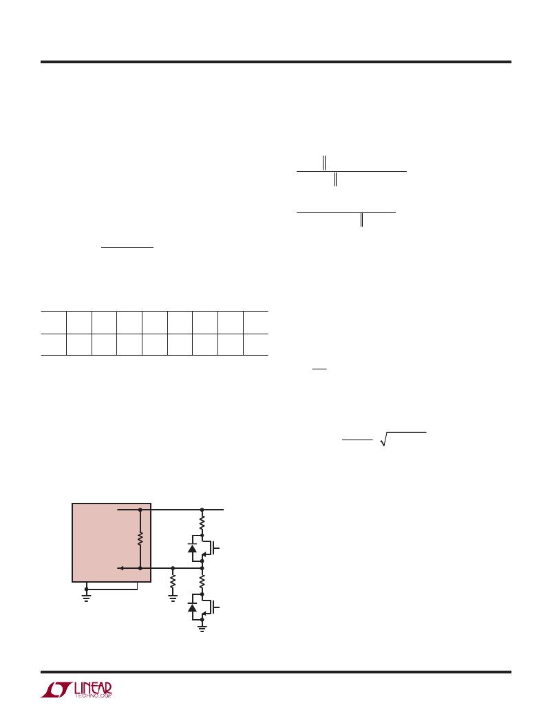
�Voltage� margining� is� the� dynamic� adjustment� of� the� output�
�voltage� to� its� worst� case� operating� range� in� production�
�D� =�
�V� O�
�V� IN�
�testing� to� stress� the� load� circuitry,� verify� control/protec-�
�tion� functionality� of� the� board� and� improve� the� system�
�reliability.� Figure� 2� shows� how� to� implement� margining�
�Without� considering� the� inductor� current� ripple,� the� RMS�
�current� of� the� input� capacitor� can� be� estimated� as:�
�function� with� the� LTM4600.� In� addition� to� the� feedback�
�resistor� R� SET� ,� several� external� components� are� added.�
�Turn� off� both� transistor� Q� UP� and� Q� DOWN� to� disable� the�
�I� CIN(RMS)� =�
�I� O(MAX)�
�%�
�?� D� ?� (1� D)�
�margining.� When� Q� UP� is� on� and� Q� DOWN� is� off,� the� output�
�voltage� is� margined� up.� The� output� voltage� is� margined�
�In� the� above� equation,� η� %� is� the� estimated� ef?ciency� of�
�the� power� module.� C1� can� be� a� switcher-rated� electrolytic�
�aluminum� capacitor,� OS-CON� capacitor� or� high� volume�
�LTM4600�
�V� OUT�
�ceramic� capacitors.� Note� the� capacitor� ripple� current�
�PGND�
�100k�
�SGND�
�V� OSET�
�R� SET�
�R� DOWN�
�Q� DOWN�
�2N7002�
�R� UP�
�ratings� are� often� based� on� only� 2000� hours� of� life.� This�
�makes� it� advisable� to� properly� derate� the� input� capacitor,�
�or� choose� a� capacitor� rated� at� a� higher� temperature� than�
�required.� Always� contact� the� capacitor� manufacturer� for�
�derating� requirements.�
�In� Figure� 18,� the� input� capacitors� are� used� as� high� fre-�
�Q� UP�
�2N7002�
�4600� F02�
�quency� input� decoupling� capacitors.� In� a� typical� 10A�
�output� application,� 1-2� pieces� of� very� low� ESR� X5R� or�
�X7R,� 10μF� ceramic� capacitors� are� recommended.� This�
�decoupling� capacitor� should� be� placed� directly� adjacent�
�Figure� 2.� LTM4600� Margining� Implementation�
�4600fc�
�9�
�发布紧急采购,3分钟左右您将得到回复。
相关PDF资料
LTM4601AHVEV#PBF
IC DC/DC UMODULE 12A 133-LGA
LTM4601AIY#PBF
IC DC/DC UMODULE 12A 133-BGA
LTM4602IV#PBF
IC DC/DC UMODULE 6A 104-LGA
LTM4603HVEV#PBF
IC DC/DC UMODULE 6A 118-LGA
LTM4603IV#PBF
IC DC/DC UMODULE 6A 118-LGA
LTM4604AIV#PBF
IC UMODULE DC/DC LV 4A 66-LGA
LTM4604IV#PBF
IC DC/DC UMODULE 4A 66-LGA
LTM4605EV#PBF
IC DC/DC UMODULE 5A 141-LGA
相关代理商/技术参数
LTM4600IVPBF
制造商:Linear Technology 功能描述:DC/DC Regulator 10A 0.6-5Vout 20Vin
LTM4601
制造商:LINER 制造商全称:Linear Technology 功能描述:Low VIN, 8A DC/DC μModule Regulator
LTM4601/
制造商:LINER 制造商全称:Linear Technology 功能描述:Low VIN, 8A DC/DC ??Module Regulator
LTM4601_12
制造商:LINER 制造商全称:Linear Technology 功能描述:LTM4601_12
LTM4601-1
制造商:LINER 制造商全称:Linear Technology 功能描述:12A DC/DC μModules with PLL, Output Tracking and Margining
LTM4601A
制造商:LINER 制造商全称:Linear Technology 功能描述:12A DC/DC μModules with PLL, Output Tracking and Margining
LTM4601A-1
制造商:LINER 制造商全称:Linear Technology 功能描述:12A DC/DC μModules with PLL, Output Tracking and Margining
LTM4601AEV#PBF
功能描述:IC DC/DC UMODULE 12A 133-LGA RoHS:是 类别:电源 - 板载 >> DC DC Converters 系列:µModule® 设计资源:VI-200, VI-J00 Design Guide, Appl Manual 标准包装:1 系列:* 类型:隔离 输出数:1 电压 - 输入(最小):66V 电压 - 输入(最大):160V Voltage - Output 1:12V Voltage - Output 2:- Voltage - Output 3:- 电流 - 输出(最大):* 电源(瓦) - 制造商系列:50W 电压 - 隔离:* 特点:* 安装类型:通孔 封装/外壳:9-FinMod 尺寸/尺寸:4.60" L x 1.86" W x 0.79" H(116.8mm x 47.2mm x 20.1mm) 包装:散装 工作温度:-25°C ~ 85°C 效率:* 电源(瓦特)- 最大:*